2023. 4. 5. 20:42ㆍEngineering
Advanced Materials Laboratory I
Synthesis and Characterization of 2D material (MoS2)
Backgrounds
What we call 2D materials are referred to as layered crystal structures, where in-plane direction lies in covalent bonding and out-plane lies in weak van der Waals force. 2D materials are unique in their properties differing from 3D materials as graphene is a well-known example. One of the charming properties of 2D materials is that the layered crystal structure is stackable. Van der Waals heterostructure formed by stacking different types of 2D materials is applicable for a 2D PN junction, a semiconductor. MoS2 is a compound 2D material that takes a significant role here.
Goal
The goal of this report is to understand the basics of 2D material synthesis. Also, recognizing the working principle of AFM and the background of Raman/PL spectra is important. Furthermore, we will compare each analyzing method in the conclusion.
Process
First, we synthesized one of the well-known 2D materials-MoS2, using mechanical exfoliation. Then, we analyzed the sample on two sides; structural and optical analysis. Structure analysis was done by Atomic Force Microscopy (AFM). Optical analysis was done by Raman and PL spectra.
Synthesis
Our experiment uses mechanical exfoliation based on the scotch-tape method for few-layer MoS2 synthesis. The bulk of the sample is grown by the CVD method. The only difference from the classical method is that we use thermal release tape for more effective exfoliation. The key to this process is to repeat attaching and detaching from tape to tape. The analysis is done by OM, AFM, and Raman measurement.
Measurements
AFM. AFM measures the surface structure by using an interaction force between the atomically sensitive tip and deflecting cantilever. The mechanism is done by detecting the laser beam (reflected by the surface of the cantilever) through a photo-diode. There exist two modes; contact mode (static mode) and non-contact mode (dynamic mode), where non-contact mode is preferred in case to prevent damage of the sample.
Raman spectroscopy. Raman spectroscopy detects the scattered monochromatic light when it hits molecules. Every material has its own Raman shift peak; therefore it is possible to distinguish its composition and vibrational state. For MoS2, there exist two types of vibration modes. Out-of-plane vibration is shown as E12g mode (383 cm-1), whereas in-plane vibration of only S atoms is shown as A1g mode (408 cm-1). These peaks are shifted and intensity changes as the layers change, therefore we get the information on the number of layers. This phenomenon is due to the change in van der Waals's interaction with layer thickness.
PL spectroscopy. When there is an absorption of light in semiconductor materials, emission can be detected eventually - This is called photoluminescence (PL). This process includes excitation, energy relaxation, and radiative recombination of electrons and holes. So, the detected light varies for each material due to the difference in band gap structure.
Experimental Result
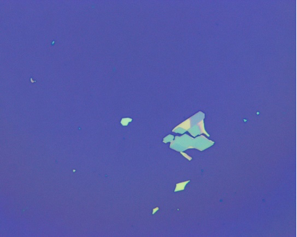
Figure 1. Observed OM image of MoS2 flake
A few-layer graphene on Si/SiO2 (300nm) substrate can be detected by OM measurement, but it is difficult when the substrate is Si/SiO2 (200nm). The reason is well explained by Blake, P. et al (2007)[1] that when Si/SiO2 Substrate is thicker, it gives a strong contrast with the graphene. Also, if the substrate is too thin, interference can appear significantly.
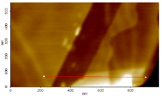

Figure 2. Monolayer profile of MoS2 flake
Max(nm) : 2.91
We analyzed the obtained image of the flake shown above. Referring to Li, X. et al (2015)[2], the general thickness of monolayer MoS2 is around 0.65 nm. From 0 to 100 nm, the layer profile is below 1 nm, which strongly supports that the layer on the left side of the image is a monolayer.
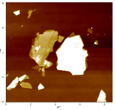

Figure 3. The thickness of MoS2 flake
Max(nm) : 0.595
This time, we analyzed a flake on the upper-right corner of a huge flake (in the middle). Again, the general thickness of monolayer MoS2 is around 0.65 nm, which is similar to our maximum layer thickness. Therefore, the flake is likely to be a monolayer.
Now we try optical analysis by using Raman and PL spectra. For the sample, the monolayer is fabricated by CVD and the multilayer is fabricated by the exfoliation method. Naturally, the fabrication method also affects the properties of the 2D material, but here we assume that the difference in properties is due solely to the difference in thickness. The data is measured at the above conditions.
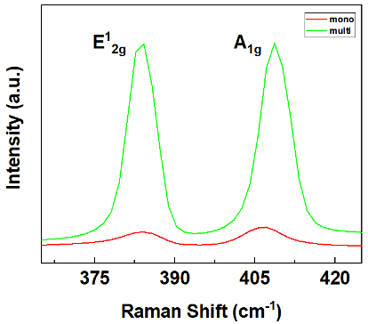
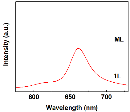
Figure 4. Raman and PL spectra of mono/multilayer MoS2 flake
The data is obtained as above. The Raman data agrees with the expectation, showing two significant peaks in E12g (383 cm-1) and A1g mode (408 cm-1). The intensity of two peaks is larger in multilayer than in monolayer. This is true because the van der Waals interaction gets stronger as the layer thickness increases. More deeply, the peak shift is recognized as the interaction changes, and the reason can be the change in interaction types. For example, interactions between the planes do not exist in a monolayer. The PL data show significant differences between monolayer and multilayer. One can notice that the intensity difference is barely observed in multilayer spectra. This can be described by the band structure of the two.
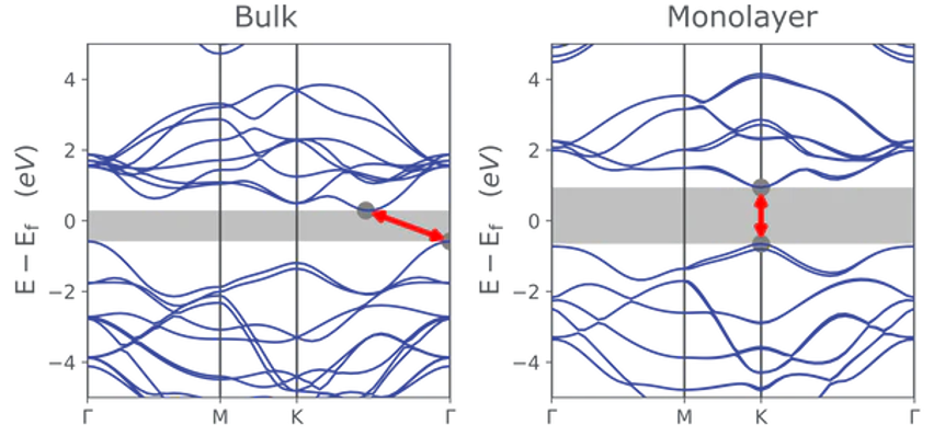
Figure 5. Band structure of MoS2 bulk and monolayer
Monolayer has a direct band gap while multilayer has an indirect band gap. For the direct band gap, the energy difference in the conduction band minimum and valence band maximum is at the same momentum. So, energy is released as a photon with a high probability when an electron in the conduction band recombines with a hole in the valence band. This results in a strong PL peak. But for an indirect band gap, the momentum differs, so the energy is released as a phonon instead of a photon. This results in a weak, broad PL peak.
Conclusion
So far, we have analyzed a mechanically exfoliated MoS2 sample with 3 methods; AFM, Raman, and PL spectra. AFM shows structural information while the remaining methods identify optical properties. Raman spectra analyze the vibrational mode by using scattered lights, showing the peak and intensity of the molecule interactions. PL spectra use the photoluminescence phenomena to analyze the band structure of the 2D materials.
References
1. Blake, P. et al. Making graphene visible. Appl. Phys. Lett. 91, https://doi.org/10.1063/1.2768624 (2007)
2. Li, X. & Zhu, H. Two-dimensional MoS2: Properties, preparation, and applications. J. Mater. 1, 33–44 https://doi.org/10.1016/j.jmat.2015.03.003 (2015)
'Engineering' 카테고리의 다른 글
| Graphene Contact Resistance 최근 동향 (0) | 2023.02.25 |
|---|---|
| Van der Waals Contact을 이용한 차세대 반도체 (0) | 2023.02.25 |
| 전자랩 : Stretchable sensors in form of serpentine structure (0) | 2023.02.24 |
| TCAD를 사용한 P-N Junction Simulation (0) | 2023.02.24 |
| 고등학교 졸업 논문 (0) | 2023.02.24 |