[전자 Lab] TCAD를 사용한 P-N Junction Simulation
Experiment objective
Simulate the basic structure of PN diode and learn parameters of PN diode. One will understand how operation properties of PN diode changes according to the parameters.
Experiment Process
1. Design of PN diode
go atlas
#Define Mesh
mesh space.mult=1
x.mesh loc=0 spac=0.1
x.mesh loc=1 spac=0.05
x.mesh loc=2 spac=0.1
y.mesh loc=0 spac=0.1
y.mesh loc=1 spac=0.1
#Define Region
region num=1 silicon x.min=0 x.max=1 y.min=0 y.max=1
region num=2 silicon x.min=1 x.max=2 y.min=0 y.max=1
#Define the electrodes
electrode name=anode x.min=0 x.max=0.1 y.min=0 y.max=1
electrode name=cathode x.min=1.9 x.max=2 y.min=0 y.max=1
#Define the doping concentration
doping uniform conc=1e16 p.type region=1
##You can change doping concentration here, by adjusting 'conc=1e16' part##
doping uniform conc=1e16 n.type region=2
#Set models, method and output
models conmob boltzman print temperature=300
##You can change temperature here, by adjusting 'temperature=300' part##
method newton trap
output band.param con.band val.band e.field
#Solve equation
solve init
save outf=pnjunction_base_nobias.str
tonyplot pnjunction_base_nobias.str
log outf=pnjunction_base.log
solve vanode=0 vstep=-0.1 name=anode vfinal=-3
solve vanode=-3 vstep=0.1 name=anode vfinal=5
log off
tonyplot pnjunction_base.log
save outf=pnjunction_base_forwardbias.str
tonyplot pnjunction_base_forwardbias.str
quit
2. Demo
1. Extract the figure of PN diode. (Using tonyplot - Structure file, plot net doping contour)

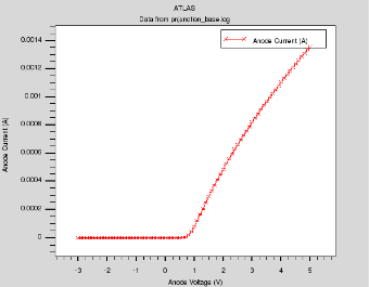
2. Extract the VAnode - IAnode. ( Using tonyplot - log file)
3. Extract band diagram with no bias.
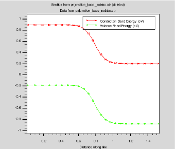
4. Extract band diagram with forward bias.

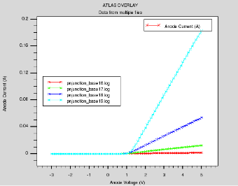
5. Repeat process 2 with various doping concentration of p region : 1E16, 1E17, 1E18, 1E19(Plot with overlay)
6. Repeat process 2 with various temperature : 200K, 300K, 400K (Plot with overlay)

'공학 > 전자공학' 카테고리의 다른 글
| [학부 연구] Graphene Contact Resistance 최근 동향 (0) | 2023.02.25 |
|---|---|
| [학부 연구] Van der Waals Contact을 이용한 차세대 반도체 (0) | 2023.02.25 |
| [전자 Lab] Stretchable Sensors in Form of Serpentine Structure (0) | 2023.02.24 |
| [전자 Lab] 스택 계산기 알고리즘 (0) | 2014.11.21 |